
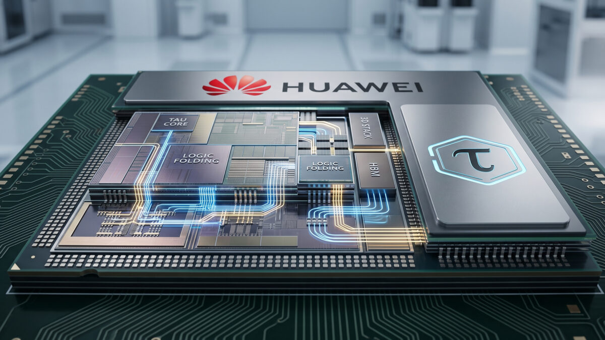
Huawei has introduced a new approach to developing advanced semiconductor chips, signalling its efforts to overcome challenges created by continuing US sanctions and restrictions on access to cutting-edge technology.
The company has proposed what it describes as a new “scaling law” for chip development, aimed at improving performance through different design methods rather than relying only on traditional techniques used in semiconductor manufacturing. The move comes as technology companies worldwide seek ways to build more powerful chips to support artificial intelligence, data processing and next-generation computing systems.
For years, the semiconductor industry has focused on making chips smaller and fitting more transistors onto them to increase speed and efficiency. However, as manufacturing becomes more complex and expensive, companies are increasingly exploring alternative methods to improve performance.
Huawei’s latest proposal reportedly focuses on restructuring how chips are designed and connected internally. Rather than depending solely on more advanced manufacturing processes, the company is looking at ways to improve computing capabilities through different architectures and system-level designs.
The announcement is being closely watched because Huawei has faced major restrictions from the United States in recent years, limiting its access to advanced semiconductor technology and manufacturing tools. These restrictions significantly affected the company’s smartphone and technology businesses and pushed it to accelerate efforts toward self-reliance.
Also Read: Tata Electronics to begin chip packaging in Assam